 Start A Project


From breadboard to production-ready.
Services / Hardware Development
Hardware development at To Be Named Labs covers the full electronics engineering scope — from schematic capture and PCB layout through component selection, BOM optimisation, and DFM review. We take hardware from a concept or rough block diagram to a production-ready design package that a contract manufacturer can build from.
We do not design hardware in isolation. Our firmware team works alongside hardware from the beginning — pin assignments, communication protocols, power sequencing, and boot behaviour are hardware decisions as much as firmware ones. Getting them wrong on a PCB costs 6–8 weeks and a respun board. We have built enough of these to know where the problems hide.
You have a validated concept and need to move from evaluation hardware (dev kits, Raspberry Pi, Arduino) to a custom PCB. You have an existing hardware design that needs a cost-down revision, a new form factor, or a compliance rework. You are a software company building your first hardware product and need someone who has done this before.
Hardware development typically follows industrial design and runs in parallel with firmware development. We recommend starting hardware and firmware together — the earlier the firmware team sees the schematic, the fewer board respins happen.
We do not design RF hardware (custom antenna design, RFIC). We do not do high-voltage power electronics or grid-connected hardware. We do not take on hardware-only engagements where the client plans to handle firmware independently — the integration risk is too high and we have seen too many projects fail at that seam.
If your product needs RF expertise or high-voltage design, we can refer you to specialists. For everything in the consumer electronics and IoT space — sensors, compute, power management, connectivity — that is our core.
KiCad and Altium Designer, depending on project requirements and client preference. We deliver in the format your contract manufacturer requires.
Yes. We work with a vetted network of PCB fabricators and contract assemblers. We can manage the manufacturing relationship end to end, or hand off the design package to your own supplier.
For a well-scoped design with a clear architecture, one to two respins is typical — one prototype build to validate function, one revision to incorporate feedback before production. We design to minimise respins, not to make them inevitable.
We design for compliance and do pre-screening in-house. For formal certification submissions, we work with accredited test labs and can manage that process on your behalf.
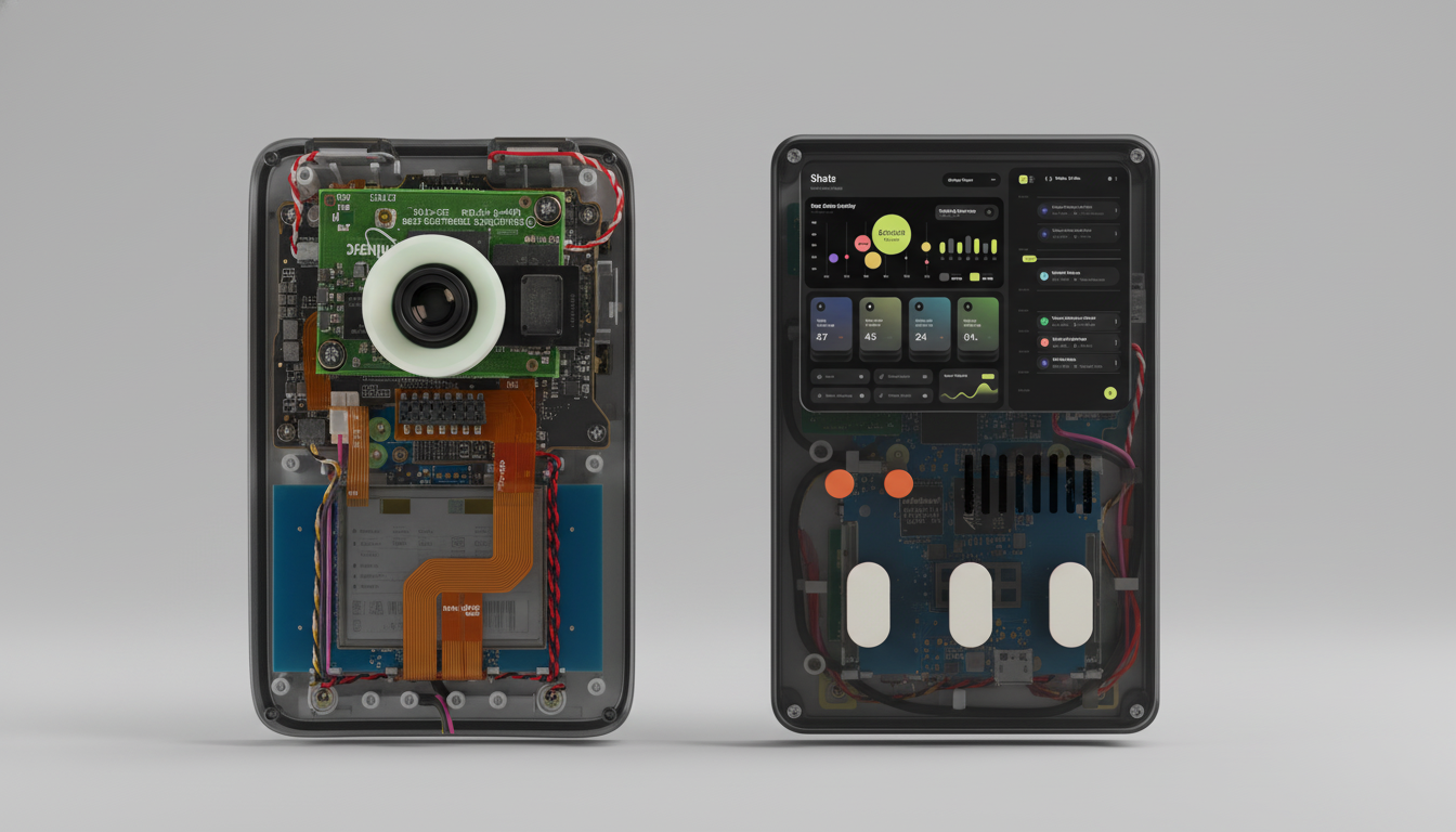
Ruggedized hardware device for industrial assembly lines. Real-time component traceability through embedded scanning and edge processing.
View case study →
Consumer electronics architects. End-to-end.